content directory
Ceramic Substrate Category
PCB substrate materials mainly include ceramic substrates, resin substrates, and metal or metal matrix composite materials. Compared with metal and resin substrates, ceramic substrates have outstanding electrical insulation properties, excellent high-frequency characteristics, and better Excellent thermal conductivity, thermal expansion rate, compatibility with various electronic components, stable chemical properties, etc., are more and more widely used in the field of substrates. Ceramic substrate products are divided into bare ceramic substrate and metallized ceramic substrate according to the production process. They are widely used as substrate materials for different thick films, thin films, and circuits. They can also be used as insulators, as heat conduction paths and in circuits with demanding thermal performance. Used to manufacture various electronic components.
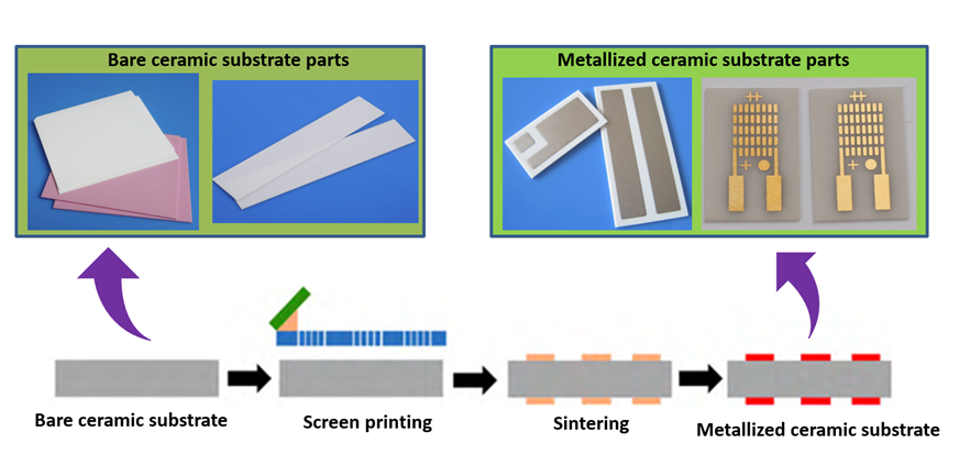
We have been producing a variety of advanced ceramic substrates for many years and have extensive manufacturing experience in Al2O3, AlN and Si3N4 materials.If customers have high precision requirements or edge processing requirements for substrate products, we can meet various requirements for size, thickness, shape and surface finish through fine grinding, polishing, laser scribing, and laser cutting processes.
We classify products into 2 types:
1) Bare Ceramic Substrate
2) Metallized Ceramic Substrate
you can find the products you need from our classification.
Bare ceramic substrate, based on electronic ceramics, is a sheet material that forms a supporting base for membrane circuit components and external components. It has high temperature resistance, high electrical insulation performance, low dielectric constant and dielectric loss, and high thermal conductivity, good chemical stability, and similar thermal expansion coefficient to components, etc., are often used as functional ceramic components in various hybrid integrated circuits, high-power modules, smart power semiconductors, automotive electronics, etc. The ceramic substrate is relatively brittle, and the substrate area is small and the cost is high. Generally, wiring, drilling, surface treatment, etc. are required.
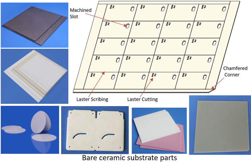
The mainstream ceramic substrates on the market include high-purity alumina ceramic substrate, aluminum nitride ceramic substrate, silicon nitride ceramic substrate and silicon carbide ceramic substrate, which have a wide range of applications and outstanding features. We specialize in tape casting and dry pressing processes to produce ceramic substrates in various standard shapes, and can also provide customized shapes through secondary processing such as laser scribing, laser cutting, and precision machining. Standard thickness includes 0.25/0.30/0.40/0.50/0.635/0.80/1.0mm etc. Additionally, custom thicknesses can be achieved if desired.
Metallized ceramic substrate, also known as ceramic circuit board, includes a bare ceramic substrate and a metal circuit layer. It refers to a special process board in which copper foil is directly bonded to the surface of a ceramic substrate (single or double-sided) at high temperature. According to the packaging structure and application requirements, ceramic substrates can be divided into two categories: planar ceramic substrates (TFC/TPC/DBC/DPC/AMB/LAM) and three-dimensional ceramic substrates (HTCC/LTCC/MSC/DAC/MPC/DMC).
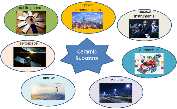
Among the planar ceramic substrates, the TFC substrate has high graphic precision, but the metal layer is thin, and is mainly used in the packaging of small current optoelectronic devices; the TPC substrate has good heat resistance, low cost, but poor circuit layer accuracy, and is mainly used in automotive sensors and other fields; DBC and AMB substrates have thicker circuit layers and better heat resistance, and are mainly used in high-power, large-temperature-changing IGBT packages; DPC substrates have the advantages of high graphic accuracy and vertical interconnection, and are mainly used in high-power LED packages; The LAM substrate meets the heat dissipation requirements of special-shaped ceramic structural parts in the aerospace field.

Among the three-dimensional ceramic substrates, HTCC/LTCC and MSC substrates are prepared by screen printing and high-temperature sintering processes, and the reliability of the cavity is high, but the accuracy of the metal circuit layer is poor; It has the advantages of high precision of the metal circuit layer and high bonding strength between the dam and the substrate, and is expected to play an important role in the fields of hermetic packaging, three-dimensional packaging and integration of power devices in the future.

The commonly used ceramic substrate materials in China are mainly Al2O3, AlN and Si3N4. Al2O3 ceramic substrate mainly adopts DBC process, AlN ceramic substrate mainly adopts DBC and AMB process, and Si3N4 ceramic substrate mostly adopts AMB process.The metallized ceramic substrate materials we produce mainly include alumina ceramics, aluminum nitride ceramics and silicon nitride ceramics. Standard thickness covers 0.25/ 0.30/0.40/0.50/0.635/1.0mm. Mainly used in LED lighting, optical communication and information equipment, medical industry, automobile industry, environment and energy industry, etc.
Performance of ceramic substrate
There is no national or industry standard for performance testing of ceramic substrates. Its main properties include mechanical properties, thermal properties, electrical properties, packaging performance (working performance) .
Mechanical properties: The mechanical properties of planar ceramic substrates mainly refer to the bonding strength of the metal circuit layer, indicating the bonding strength between the metal layer and the ceramic substrate, which directly determines the packaging quality of subsequent devices (die bonding strength and reliability, etc.). The bonding strength of ceramic substrates prepared by different methods is quite different. Generally, planar ceramic substrates (such as TPC, DBC, etc.) prepared by high-temperature processes have a high bonding strength between the metal layer and the ceramic substrate through chemical bonds; while those prepared by low-temperature processes For ceramic substrates (such as DPC substrates), the van der Waals force and mechanical occlusal force are mainly used between the metal layer and the ceramic substrate, and the bonding strength is low.
Thermal properties: The thermal properties of ceramic substrates mainly include thermal conductivity, heat resistance, thermal expansion coefficient and thermal resistance. The ceramic substrate mainly plays the role of heat dissipation in the device package, so its thermal conductivity is an important technical index; the heat resistance mainly tests whether the ceramic substrate is warped and deformed at high temperature, and whether the surface metal circuit layer is oxidized, discolored, blistered or peeled off. layers, whether internal vias fail, etc. Since the ceramic substrate is generally a multi-layer structure, its thermal conductivity is not only related to the thermal conductivity of the ceramic substrate material (bulk thermal resistance), but also closely related to the bonding of the material interface (interface contact thermal resistance). Therefore, using a thermal resistance tester (which can measure bulk thermal resistance and interface thermal resistance of multilayer structures) can effectively evaluate the thermal conductivity of ceramic substrates.
Electrical properties: The electrical properties of ceramic substrates mainly refer to whether the metal layers on the front and back of the substrate are conductive (whether the quality of the internal through holes is good). Due to the small diameter of the through hole of the DPC ceramic substrate, there will be defects such as unfilled holes and pores during electroplating and filling. Generally, X-ray testers (qualitative, fast) and flying probe testers (quantitative, cheap) can be used to evaluate ceramic substrates. Via quality.
Packaging performance: The packaging performance of ceramic substrates mainly refers to solderability and air tightness (limited to three-dimensional ceramic substrates).
Solderability refers to whether the chip or metal lead can be successfully welded (bonded) with the substrate metal layer, and has a certain bonding strength. In order to improve the solderability of the ceramic substrate, it is generally necessary to carry out surface treatment on the metal layer of the substrate (such as electroless silver plating, electroless Ni/Au, Ni/Pd/Au, etc.), which can prevent the oxidation of the metal layer and improve the solderability of the metal layer . The composition and thickness of the surface treatment layer has a great influence on solderability, which can usually be evaluated by using a wire bonder and a shear strength tester.
The chip is mounted in the cavity of the three-dimensional ceramic substrate, and the cavity is sealed with a cover plate (metal or glass) to realize hermetic packaging of the device. The airtightness of dam materials and welding materials directly determines the airtightness of device packaging, and there are certain differences in the airtightness of three-dimensional ceramic substrates prepared by different methods. For three-dimensional ceramic substrates, the airtightness of dam materials and structures is mainly tested, mainly including fluorine oil bubble method and helium mass spectrometer method.
Testing of ceramic substrate
Appearance inspection: The appearance inspection of ceramic substrates generally uses the naked eye or microscope to detect whether there are cracks and holes on the surface of the substrate, and whether there are quality defects such as bubbles, delamination, scratches or stains on the surface of the metal layer. In addition, the size of the ceramic substrate, substrate flatness (warpage), metal circuit layer thickness and surface roughness, line width and spacing, etc. are all important inspections.
Common bond strength testing methods include:
(1) Adhesive tape method: stick 3M adhesive tape to the surface of the metal layer, and roll it with a rubber roller to remove air bubbles in the bonding surface. After 10s, use a pulling force perpendicular to the metal layer to peel off the tape to detect whether the metal layer is peeled off from the substrate, which is a qualitative test method.
(2) Wire welding method: select a metal wire with a diameter of 0.5 mm or 1.0 mm, and directly weld it on the metal layer of the substrate through solder melting, and then measure the tensile force of the metal wire along the vertical direction with a tensile gauge.
(3) Peel strength method: Etch (cut) the metal layer on the surface of the ceramic substrate into 5 mm x 10 mm strips, and then tear it off in the vertical direction on a peel strength testing machine to test its peel strength. The peeling speed is required to be 50mm/min, and the measurement frequency is 10 times/s.
Commonly used test methods include shear strength test and tensile strength test as follows.
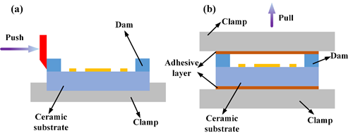
Reliability Testing and Analysis :Reliability mainly tests the performance changes of ceramic substrates in specific environments (high temperature, low temperature, high humidity, radiation, corrosion, high frequency vibration, etc.), the main contents include heat resistance, high temperature storage, high and low temperature cycle, thermal shock, corrosion resistance , corrosion resistance, high frequency vibration, etc. For failed samples, scanning electron microscope (SEM) and X-ray diffractometer (XRD) can be used for microcosmic and component analysis respectively; scanning acoustic microscope (SAM) and X-ray detector can be used for welding interface and defect analysis.
Ceramic substrate application
1. Packaging of power electronic devices:
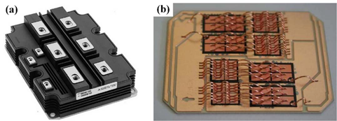
Since the 1950s, power electronic devices have transitioned from thyristors to GTR/GTO/MOSFETs, and then gradually developed to Insulate-Gate Bipolar Transistor( IGBT). Compared with the previous two generations, the third-generation power electronic devices (such as IGBT) have the advantages of high frequency, high power and fast switching speed. be widely used. Due to the high output power of IGBT and large heat generation, poor heat dissipation will damage the IGBT chip. Therefore, for IGBT packaging, heat dissipation is the key to its technology, and ceramic substrates must be used to enhance heat dissipation. At present, DBC ceramic substrates are mainly used for IGBT packaging. The reason is that the metal circuit layer of DBC substrates is relatively thick (generally 100 μm ~ 600 μm), which has the characteristics of large current carrying capacity, good high temperature resistance and high reliability.
As shown in the figure: (a) IGBT module and (b) use DBC substrate to package IGBT module.
2. Laser (LD) package:
LD is a semiconductor device of stimulated radiation, widely used in industry, military, medical and 3D printing and other fields. At present, the output power of commercial products of 90μm~100μm single-tube 9××nm devices in the world is between 12W~18W, and the laboratory level can reach 20W~25W. Since the electro-optical conversion efficiency of LD is about 50%~60%, a large amount of heat is concentrated in the active area during operation, resulting in an increase in junction temperature, causing catastrophic optical damage or saturation on the cavity surface, and severely limiting the output power and service life of the LD. In addition, the mismatch of thermal expansion coefficients leads to thermal stress inside the device, and the output light is distributed nonlinearly in the fast axis direction, which brings great challenges to beam collimation, shaping and fiber coupling, and is one of the main factors hindering the wide application of high-power lasers. one.
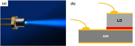
Therefore, ceramic substrates with good thermal conductivity and matching thermal expansion coefficients must be used in LD packages. Because AlN ceramics have the advantages of high thermal conductivity and low thermal expansion coefficient, AlN ceramic substrates are commonly used in LD packages.
As shown in the figure (a) blue light LD device and (b) schematic diagram of LD packaged with DBC substrate.
3. Light Emitting Diode (LED) Packages:
Like LD, light-emitting diode (LED) is also a semiconductor power device based on electro-optic conversion. It has the advantages of high electro-optic conversion efficiency, fast response, long life, energy saving and environmental protection. It has been widely used in general lighting, signal indication, automotive lamps and lanterns. And backlight display and other fields. With the development of LED technology, chip size and driving current continue to increase, and the power density of LED modules also continues to increase, and the problem of heat dissipation is becoming more and more serious.
High-power LED packaging substrates have gone through three stages: metal brackets, metal substrates and ceramic substrates. Due to the characteristics of ceramic substrates such as high insulation, high thermal conductivity, heat resistance, and low expansion, especially the DPC ceramic substrate with vertical through-hole technology, it can effectively meet the requirements of flip-chip eutectic, COB (chip on board), CSP (chip size) packaging) and other technical white light LED packaging requirements.
Schematic diagram of the white LED module and its ceramic package as shown.

For UV LED modules, three-dimensional ceramic substrates are used to meet their high-efficiency heat dissipation and airtight packaging requirements.As shown in the figure, the UV LED module and its packaging structure.

4. Thermoelectric cooler (TEC) package:
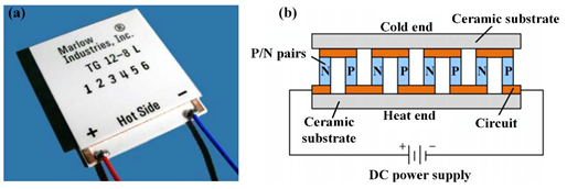
Thermoelectric Cooler (Thermoelectric Cooler, TEC) is a commonly used semiconductor cooling device, and its working principle is the Peltier effect. The advantages of thermoelectric refrigeration technology are obvious, mainly in: (1) no moving parts, no noise, no wear, long life, easy to control, high reliability; (2) no refrigerant, no leakage, no pollution to the environment; ( 3) The refrigerator is small in size and light in weight, and is suitable for heat dissipation of electronic devices in special environments such as small volume and small size. Since the thermoelectric cooling efficiency is positively correlated with the number of semiconductor particles, the more particles per unit area, the higher the thermoelectric cooling efficiency. The DPC ceramic substrate has high graphic precision, which can increase the density of particle arrangement, thereby effectively improving the efficiency of thermoelectric cooling.
As shown in the figure, the thermoelectric cooler sample and the schematic diagram of the thermoelectric cooler package.
5. High temperature electronics (HTE) packaging:
Electronic devices in aerospace, deep-sea drilling, automotive and other fields need to be able to work in extreme environments (such as high temperature, high humidity, high pressure, high corrosion, high radiation, high frequency vibration, etc.), so packaging materials must have high heat resistance and resistance Moisture, and the device chip must be sealed in the cavity to avoid erosion and damage from the external environment. The aforementioned three-dimensional ceramic substrates (such as HTCC, LTCC, MPC, and DMC, etc.) have a high-strength cavity structure and good airtightness, which can meet the requirements of device packaging in harsh environments.
As shown in the figure, the crystal oscillator with LTCC hermetic package and its package structure diagram.

6. Other power device package:
Ceramic substrates are also used in many other power or high temperature device packages due to their good thermal conductivity, heat resistance and reliability. Such as focused photovoltaic device packaging, due to the increase of sunlight density due to the focusing effect, the chip temperature rises, and ceramic substrates must be used to enhance heat dissipation. In addition, in the field of microwave radio frequency, in order to reduce loss, it is necessary to use HTCC or LTCC substrate with good high-frequency characteristics to increase the speed.

